As a leading wide bandgap semiconductor manufacturer, ON Semiconductor is a pioneer in this technology and creating one of the lowest RDSon SiC MOSFETs. We offer best-in-class packaging technology, a comprehensive range of energy-efficient power solutions, including advanced Silicon Carbide (SiC) based devices such as SiC MOSFETs, SiC Diodes, SiC and GaN drivers and integrated modules.
ON Semiconductor has expanded its range of wide bandgap (WBG) devices with the introduction of two new families: 1200 volt (V) and 900 V N-channel SiC MOSFETs. With the introduction of this technology, discover the use cases for the new SiC MOSFET’s we have introduced, as well as what end applications will benefit the most with our new SiC solutions.
1200 V SiC MOSFETs
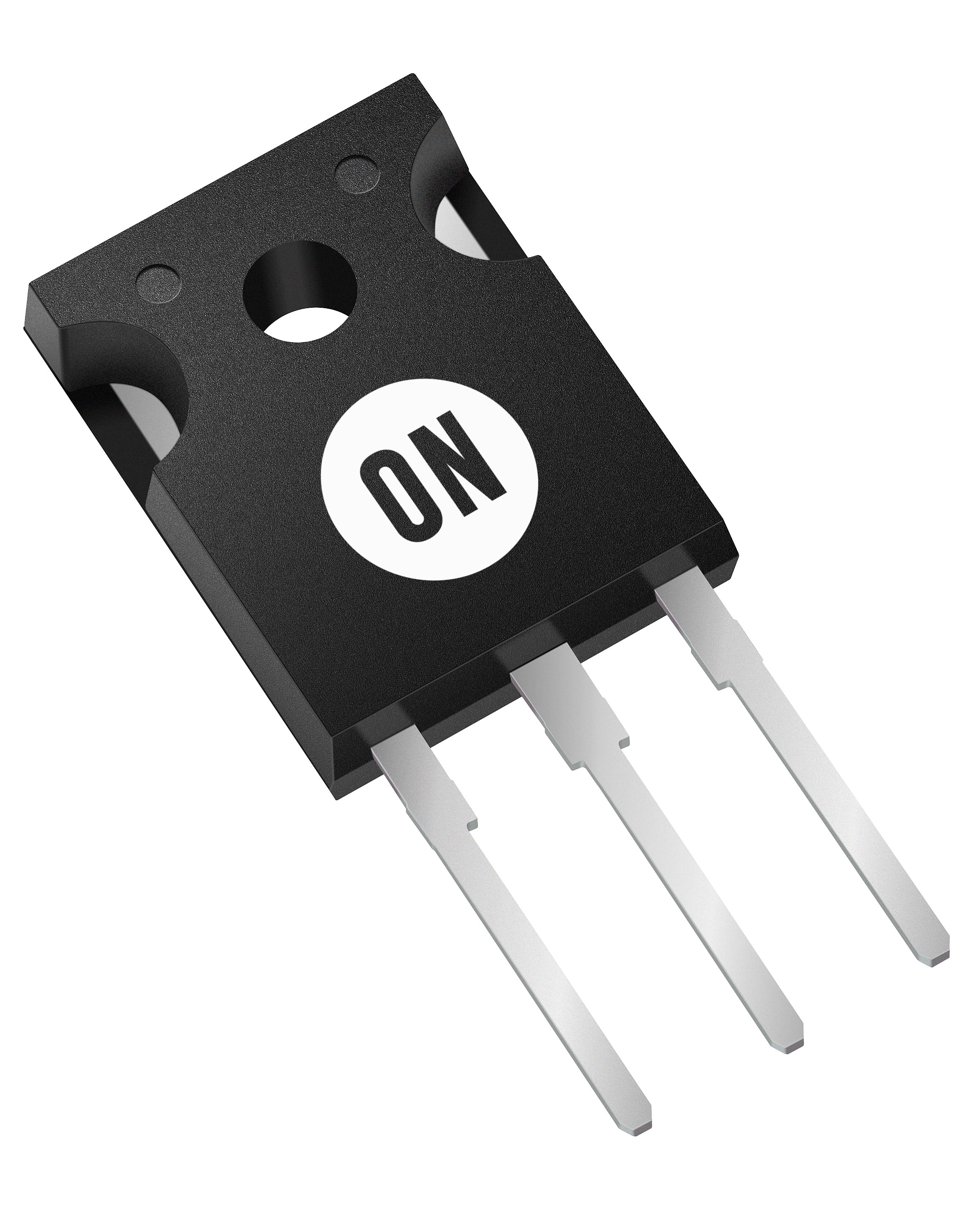
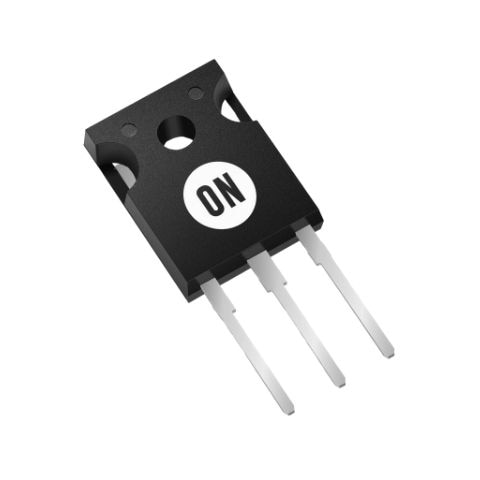
Q: What is the major characteristic of the NTHL020N120SC1, SiC Carbide MOSFET, N‐Channel, 1200 V, 20 mΩ?
A: The NTHL020N120SC1 was designed to provide extremely low conduction losses with a blocking voltage (VDSS) of 1200V. In addition, it was designed to drive fast with low internal gate resistance (Rg = 1.81Ω) and low output capacitance (Coss = 260pF).
Q: Compared to existing ON Semiconductor SiC MOSFETs (prior to releasing the NTHL020N120SC1), what characteristics were improved in the NTHL020N120SC1?
A: This is our first generation of SiC MOSFETs so we cannot compare to previous devices. However, our devices have some advantages over other devices on the market – strong oxide performance (VGS rating +25V/-15V), no Vth drift, no body diode drift, high switching speed, smooth gate drive with dv/dt control and strong body diode for hard switching.
Q: What are competitive specs the NTHL020N120SC1 offers?
A: Our 1200V SiC MOSFET devices are very competitive in the market, meeting or beating most customer specs. Each application cares about different parameters, but in general, we designed our parts to operate quickly, reducing switching and conduction losses. We did this by achieving a low RDSon, as well as choosing a low internal gate resistor for fast switching. We have designed the devices to be rugged with fast transient immunity capable of over 100V/ns.
Q: What are the advantages of SiC?
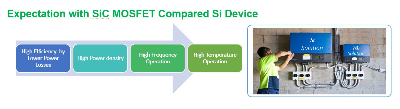
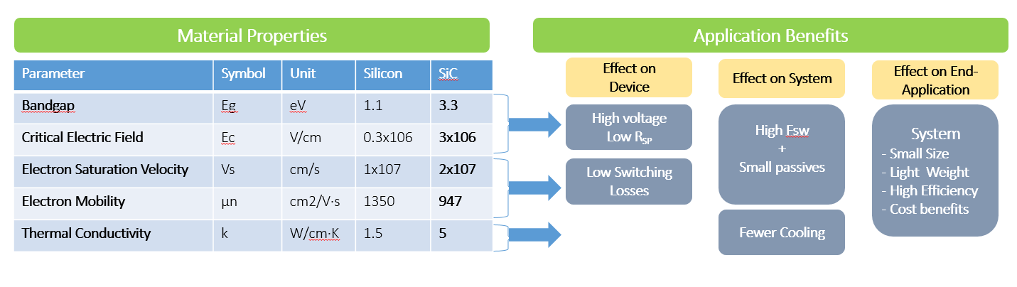
A: The advantage of SiC starts in the material itself having a 10x higher dielectric breakdown field strength, 2x higher electron saturation velocity, 3x higher energy band gap and 3x higher thermal conductivity than Silicon. System benefits offer the highest efficiency by lowering power loss, greater power density, higher operating frequency, increased temperature operation, reduced EMI and most importantly, reduced system size and cost.
End Applications:
Q: What is an end application that will fully utilize the major characteristic of the NTHL020N120SC1?
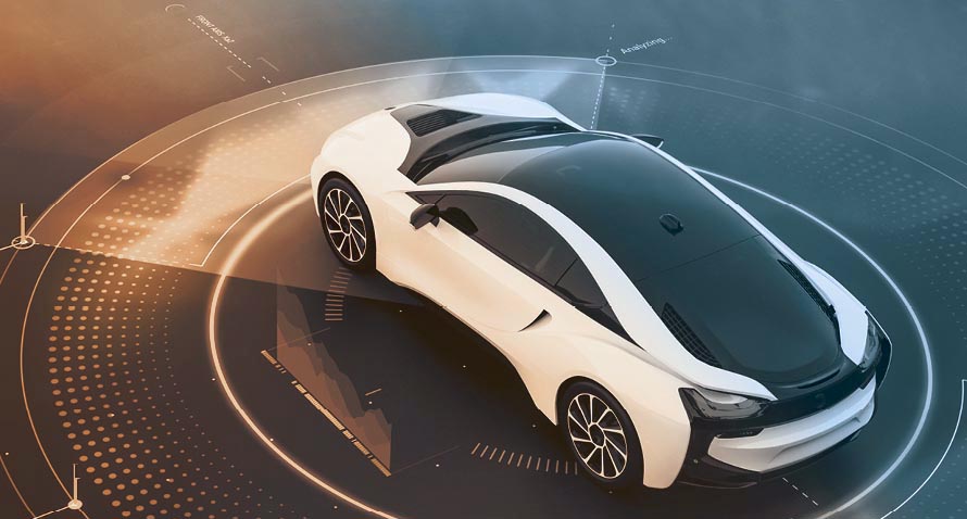
A: A wide variety of end applications will benefit significantly by reducing BOM content as well as increasing power density. Two specific applications where this is evident is in solar power inverters as well as electric vehicle (EV) charging stations.
Q: Why does the SiC MOSFET product especially benefit solar power inverters and electric vehicle charging stations? Do those applications have strong requirements of size/form factor? If so, could you please tell us the background or needs?
A: Traditionally most PFC stages are complex, have limited frequency and have never achieved more than 98% efficiency. Using SiC allows fewer components (less complex), smaller passives, better cooling, as well as greater than 98% efficiency.
Q: Is there a great demand for smaller solar power inverters and charging stations? And if so, what are the reason?
A:
Solar Inverters:
There are currently two trends in the solar inverters market space. ON Semiconductor has an estimated 30% share of the market TAM.
1) Multiple small inverters < 20kW for each row of panels that convert the DC to AC and then feed into a big megawatt inverter
- The small < 20kW inverters typically are moving to discrete SiC for the PCF stage. For LLC it is a mix of SJ and SiC depending on the timeline, cost and efficiency targets.
- If the customer moves to SiC, there are many advantages but the gate drive voltage is higher so that is a drawback the circuit has to be re-designed.
2) A few larger inverters > 20kW that take multiple rows of panels and don’t feed into a bigger one
- The bigger inverters > 20kW are typically using power modules.
- Previously these were IGBT modules, then it moved to hybrid modules the last 5 years (IGBT + SiC Diode), now we are seeing SiC MOSFET modules being used.
Charging Stations:
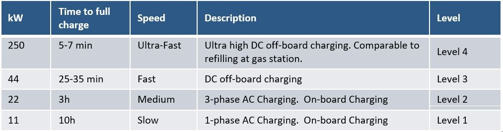
Charging stations have 4 levels of power levels. Levels 1 and 2 are 1/3 phase AC chargers. These chargers do not use SiC and use a car’s OBC to charge the battery. Levels 3 and 4 are higher power and use AC/DC on the charging pole, so when you connect to a car it charges the battery directly.
In addition, we classify 3 “market” segments within charging stations
1) Residential – level 1 or 2 charger
2) Commercial – level 2 or 3 (mall, work, somewhere the car is parked for a bit)
3) Highway – level 3 or 4 (this is where SiC will be used)
In general, the charging market is especially high power is still developing. Here we see a majority of it being power modules due to the high power but see some discrete on the LLC or secondary rectification stage.
Learn more about ON Semiconductor’s wide bandgap solutions and advantages today!
Be sure to subscribe to our blog and follow us on social media to receive the latest updates on our technologies, solutions and company news!
Twitter | Facebook | LinkedIn | Instagram | YouTube