Providing electrical isolation is often essential in power system designs; keeping high and low voltage domains electrically separate prevents current flowing between them, which could otherwise lead to serious safety issues. Of course, it is still necessary and possible for isolated domains to interact, by allowing data to pass between them.
Though isolation is commonplace, implementing it effectively can still be problematic, especially as we move to ever greater levels of system integration. Its primary purpose is safety, but it can also improve performance by maximizing common mode transient immunity (CMTI), which is one of the main reasons why isolation is used in the automotive industry. Another reason, particularly in electric vehicles, is to support power conversion and level shifting between voltage domains.
Power conversion systems generally use power MOSFETs or IGBTs. These devices require gate drivers to switch them on and off, using low voltage signals. This is a typical example of where isolation is needed to keep the different voltage domains separate but connected. Isolation is typically implemented using optocouplers, which requires at least two discrete devices; the emitter, which is an LED and the receiver, which includes a photodiode.
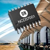
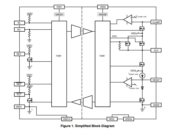
Although optocouplers can easily achieve very high isolation of 5 kVrms and above, they are bulky and prone to aging. It is possible to achieve communication across the isolation barrier without light, while still preserving the isolation levels needed. The optocoupler can be ideal in many applications, but there is also a trend towards alternative technologies for integrated isolation devices that offer even more convenience. One example is the NCD57001 from ON Semiconductor. It uses magnetic coupling through a coreless transformer to create a data path between microfabricated inductors, providing 5kVrms of galvanic isolation and a minimum of 100kV/us CMTI.

Figure 1: An NCD57001 Advanced Gate Driver IC from ON Semiconductor
Another notable feature of the NCD57001, developed specifically to address a common issue, is its output stage. It features an internal buffer stage that is designed to overcome the Miller Plateau. This is the region on the transfer curve that proves the undoing of many gate drivers. During this period, the parasitic Miller capacitance takes effect, with the result of slowing down the on/off transition speed.

To compensate for the slugging effect of the Miller Capacitance, the output buffer has the job of boosting the drive current, through the Miller Plateau. The Miller Capacitance on the gate terminal is responsible for a significant proportion of switching losses. By providing high current output drive as the gate voltage starts to rise and the difference between the driver output voltage and gate voltage falls, the IGBT or MOSFET moves through the Miller Plateau quicker. It achieves this by using the output stage's boosting effect to reduce the time needed to charge the parasitic/Miller gate capacitance.
Through its coreless transformer technology, the NCD57001 provides effective isolation in chip-level gate drivers. These fully integrated, isolated gate drivers offer real engineering benefits and provide a great alternative to opto-isolated drivers in applications that need high levels of isolation in a small format. With its output boost stage, designed to overcome the Miller Plateau, it also improves switching efficiency. As more applications adopt high DC voltages, the need for efficient and safe isolation is growing. This is where innovative solutions like the NCD57001 can really make a positive difference to your next power switching application.
Learn more about the NCD57001 high current gate driver via our application note and discover our comprehensive gate driver solutions.
Be sure to subscribe to our blog and follow us on social media to receive the latest updates on our technologies, solutions and company news!
Twitter | Facebook | LinkedIn | Instagram | YouTube
